


Dr. Manish Goswami

At present there is no content available for this section, once content will be available would be updated.
ASIC Implementation of Low Power Variable Resolution ADC
High-resolution ADCs typically consume significant power and occupy large silicon area. To address this, we designed an ADC that detects current operating conditions and adjusts its resolution dynamically.
In this design, the resolution is varied based on channel conditions. Power saving is achieved by switching certain ADC stages to standby mode, where only leakage current contributes to power dissipation.
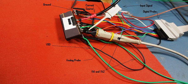
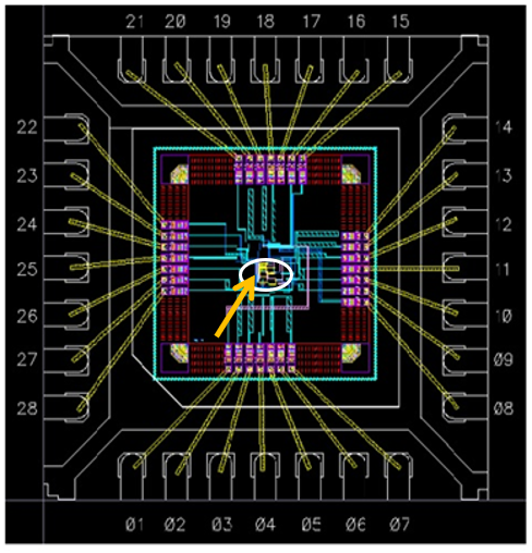
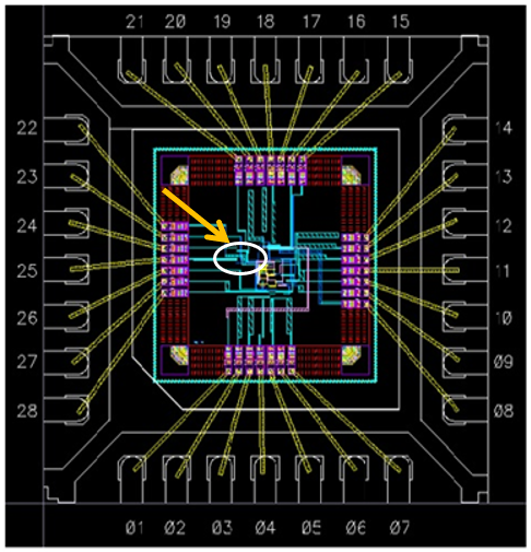
The variable resolution ADC was designed using the Tanner Tool on 500nm CMOS technology (AMIS_0.5_CFN kit), and was fabricated at the MOSIS foundry. This marks the first chip fabricated by our group at IIIT-A.
This work has also been extended to a Binary Search ADC design.
A Reusable Stage Based Reduced Comparator Count Binary Search ADC
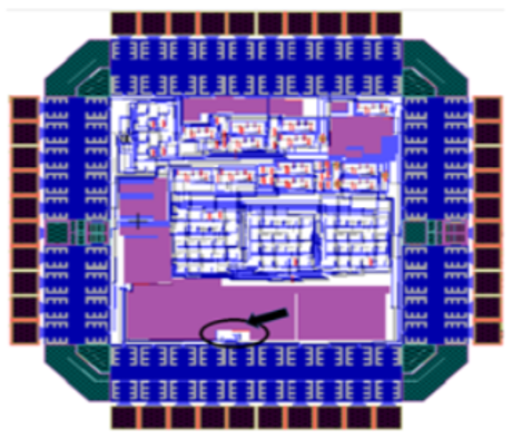
This design implements a reduced-comparator-count Binary Search ADC using a reusable stage-based architecture. The chip has been fabricated using SCL 180nm CMOS technology.
True Random Number Generator Using Jitter, Metastability, and Current-Starved Topology
This chip, fabricated at SCL using 180nm technology, employs jitter, metastability, and current-starved topology for true randomness. The randomness was validated using the NIST Test Suite, which defines various statistical properties of random sequences.
The proposed design achieved a very high pass efficiency.
7T SRAM Cell Using Supply Feedback Technique
This design demonstrates a 7T SRAM cell using a supply feedback technique. It was fabricated using MOSIS (AMIS) C5X, 1P-2M CMOS process.
At present there is no content available for this section, once content will be available would be updated.
- Back to previous page
- |
-
Page last updated date:22-07-2025 01:15 PM


